MSM XX
MSM XX
The 20th Microscopy of Semi Conducting Materials will take place in Oxford in 2017.
The conference will focus on the most recent advances in the study of the structural and electronic properties of semiconducting materials by the application of transmission and scanning electron microscopy. The latest developments in the use of other important microcharacterisation techniques including scanning probe microscopy, X-ray topography and diffraction will also be featured.
Developments in materials science and technology covering the complete range of elemental and compound semiconductors will be described.
Registration has now closed. If you have any queries please contact Karina Lang.
Provisional programme
Speakers
Scientific Organisers
-
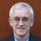
Dr Thomas Walther
University of Sheffield
Thomas is Reader in Advanced Electron Microscopy at the University of Sheffield and Director of the Kroto Centre for High Resolution Imaging and Analysis.
His research areas include electron microscopy method development and instrumentation, in particular HREM, EFTEM, ADF-STEM, EELS, ELNES, EDX.
A focus is on quantitative analysis of semiconductor quantum wells and quantum dots, but also the study of interdiffusion and segregation at grain boundaries and within metal nano-particles.
He runs the Microscopy of Semiconducting Materials conference series which is alternatingly held in Oxford and Cambridge, always in odd years. -

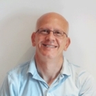
Dr Lewys Jones FRMS
University of Dublin
After a first degree in Material Science, I received my PhD from the Department of Materials at the University of Oxford in 2013. This focussed on two themes; scanning stability in the aberration-corrected scanning transmission electron microscope (AC-STEM) and also on applications of focal series of annular dark-field data. In 2014 a software plug-in for Digital Micrograph to correct scan-noise (the Jitterbug software) was launched in collaboration withHREM Research. More recently in 2016, another plug-in to bring fast non-rigid registration to DM was launched (SmartAlign).
I sit on the Editorial Board of the journal Advanced Structural and Chemical Imaging, and have been a Fellow of the Royal Microscopical Society since 2015.
Invited Speakers
-
Prof Ken Durose
University of Liverpool, UK
Ken Durose is Professor of Applied Physics at the University of Liverpool where he is Director of the Stephenson Institute for Renewable Energy. He was educated at Durham University, receiving his PhD in 1987 after which he worked at British Telecom Research Labs on laser photochemical processing for III-V communication devices. Thereafter he took up a faculty position at Durham and developed interests in the microstructure of II-VI semiconductors and crystal growth. This was an ideal starting point for joining EU programmes on solar photovoltaic materials and solar cells, and he developed interests in device fabrication and the mechanisms by which the efficiencies are limited - including by both extended and point defects. This work on CdTe devices was expanded to include growth and doping studies on transparent conductors and also new and sustainable materials and devices for photovoltaics, including complex chalcogenides and hybrid perovskites. He was principal investigator of the UK PV programme for two cycles from 2004 – 2012 and is presently Director of the EPSRC Centre for Doctoral Training in New and Sustainable PV. He has been a Fellow of the RMS since 1989. -
Prof Jaime Gomez-Rivas
Eindhoven University of Technology, the Netherlands
Jaime Gómez Rivas studied Physics and Astrophysics at the Universidad Complutense of Madrid (Spain) and at the Université de Liege (Belgium). In 2002 he received the PhD degree at the University of Amsterdam (The Netherlands) for his research on Anderson localization of light. He worked as postdoctoral researcher at the RWTH University in Aachen (Germany) from 2002 until 2005 on THz photonics and plasmonics. In 2005 Gómez Rivas become project leader at the FOM Institute for Atomic and Molecular Physics, AMOLF, in Amsterdam and at Philips Research in Eindhoven (The Netherlands), setting up the group Surface Photonics working on nano- and THz-photonics. In 2010 he was appointed as part-time professor at Eindhoven University of Technology (TU/e) and group leader at AMOLF. In 2015 Gómez Rivas moved with his group to the Dutch Institute for Fundamental Energy Research in Eindhoven and he became full-professor at TU/e. Gómez Rivas is co-author of over 120 publications in peer-reviewed journals and co-inventor of 20 patents and patent applications. -

Prof James Lebeau
North Carolina State University, USA
James earned his B.S. in Materials Science & Engineering from Rensselaer Polytechnic Institute in 2006 and his Ph.D. from the University of California Santa Barbara in 2010. After his graduate work, he joined the Department of Materials Science and Engineering at North Carolina State University as a faculty member in 2011 and was promoted to Associate Professor in 2016. His research focuses on applying and developing transmission electron microscopy techniques to determine the atomic structure and chemistry of materials. For his research, James has been honored with numerous awards including the NSF CAREER award and the AFOSR Young Investigator grant. He has been recognized by the Microanalysis Society with a Distinguished Scholar award, the Birks Award, and the K.F.J Heinrich award recognizing a scientist under the age of forty for distinguished technical contributions in the field. Most recently, his work was selected for a 2016 Best Paper award in the journal Microscopy and Microanalysis. Since 2006, he has co-authored over 60 journal articles, which have been cited over 1500 times. -
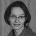
Dr Anna Mogalitenko
Ferdinand Braun Institute, Germany
Anna Mogilatenko has studied Materials Science and obtained an Engineer Degree (Dipl.-Ing.) at National Technical University of the Ukraine in Kiev. Her PhD (Physics Department of Chemnitz University of Technology, Germany) was focused on transmission electron microscopy analysis of thin silicide films. As a postdoc at Humboldt University of Berlin she started analysing group-III nitride materials. Her current research interests at Ferdinand-Braun-Institute include analysis of defect distributions and compositional changes in AlGaN-based heterostructures. This allows for understanding, developing and improving of devices like photodetectors and light emitting and laser diodes operating in the ultraviolet wavelength range. The applied analyses techniques include diffraction contrast analysis, HAADF STEM, CBED, HRTEM, EDXS and EELS as well as CL in SEM. -
Prof Yutaka Ohno
IMR Tohoku University, Japan
I am working in the Physics of Crystal Defects division in IMR as an associate professor (http://lab-defects.imr.tohoku.ac.jp/ohno/ohno.html). A focus is on quantitative analyses of the impurity segregation ability of grain boundaries in Si and compounds by atom probe tomography (with an impurity detection limit less than 0.005 at.% on a boundary simultaneously with a spatial resolution less than 0.4 nm) combined with HAADF-STEM and ab-initio calculations, but also the study of atomistic structures of semiconductor nanostructures by optical measurements (CL, PL, SNOM) under TEM. -
Dr Pierre Ruterana
CIMAP ENSICAEN, France
Dr. Pierre Ruterana is Doctor es Science in Materials Science. His is Director of Research in CNRS (French National Centre for Scientific Research). He is Head of the Research TEAM "Properties of materials for energy savings" PM2E in Laboratory CIPAM (Centre de Recherche sur les Matériaux, les Ions et la Photonique). Dr Ruterana is specialist in high resolution electron microscopy with applications to numerous materials including semiconductors, ceramics, catalysts and nanomaterials. He joined CNRS in 1991, since then he has trained some 20 PhD students, collaborated in many national and international projects, coordinating most of them. He has contributed to more than 300 scientific publications in peer reviewed journals, and delivered more than 70 invited talks at international conferences. Up to now, he has been the principal organiser of more than 10 workshops and/or symposia at international conferences. -

Dr Ana Sanchez
University of Warwick, UK
Ana is Principal Research Fellow at the University of Warwick. Her research interests are based on developing the field of advanced transmission electron microscopy techniques and materials characterization, mainly in the areas of semiconductors (including 2D dichalcogenides) and ferroelectric materials. She has been collaborating with world-leading groups using advanced microscopy techniques both to determine defect structure in materials and the challenging and technologically relevant problem of determining strain and composition at nanometer scale. -
Prof Takashi Sekiguchi
National Insitute of Materials Science, Japan
Takashi Sekiguchi has been engaged in the study of defects in semiconductors using cathodoluminescence and EBIC for 30 years and published more than 400 papers. His started this work on the dislocation related luminescence in Si. Then, he has been studying wide variety of materials from multicrystalline Si for solar cells, widegap semiconductors like GaN and SiC, III-V quantum structures, and various types of nanoparticles. -
Prof Kerstin Volz
Universitat Marburg, Germany
Prof Kerstin Volz is full Professor for Experimental Physics and Co-Leader at the STRL (Structure and Technology Research Lab) of Philipps University Marburg since 2009.
She received her diploma in physics from Augsburg University in 1996. In 1999 she obtained her PhD from the same university. After several research visits at Osaka National Research Institute and Nagasaki Institute of Technology in Japan, as well as a postdoctoral stay at Stanford University, she joined Philipps-Universität Marburg as a Junior Group Leader (in the framework of a Topical Research Group of the DFG). After a professorship at the Humboldt-Universität of Berlin, she was appointed as a Heisenberg professor in Marburg.
She presently serves there as speaker of the Research Training Group “Functionalization of Semiconductors”, which started in 2012. She is also the vice-coordinator of the collaborative research center “Structure and Dynamics of Internal Interfaces”. She has received the following awards: Graduate Student Award of EMRS (1996); Feodor-Lynen scholarship of Alexander von Humboldt foundation (2001); guest professorship of Humboldt Universität of Berlin (2008); Heisenberg professorship of DFG (2008); and the Patricia Pahamy Prize for best teaching (2009). Her research interests include the synthesis (MOVPE) and quantitative transmission electron microscopy of novel functional materials. -
Prof Qihua Xiong
Nanyang Technological Univeristy
Qihua Xiong received his B.S. degree in physics from Wuhan University in 1997, and then finished three years graduate studies at the Shanghai Institute of Applied Physics, Chinese Academy of Sciences. He went to the United States in 2000 and received Ph.D. degree under the supervision of Prof. Peter C. Eklund from The Pennsylvania State University in 2006. After three years postdoctoral experience in Prof. Charles M. Lieber’s group at Harvard University, he joined Nanyang Technological University as an assistant professor in 2009 and promoted to Nanyang Associate Professor in 2014. He was promoted to full Professor in 2016 recently. He is a Fellow of Singapore National Research Foundation awarded in 2009 and the inaugural NRF Investigatorship Award by Singapore National Research Foundation. Prof. Xiong’s research focuses on light-matter interactions of emergent quantum matter by optical spectroscopy approaches. He recently ventured into the field of 2D layered materials and laser cooling of solids. -
ProfHongzhou Zhang
Trinity College Dublin
Prof Zhang received his PhD in Applied Physics at Rice University (US) in 1999. He worked as a Research Fellow at the Australian National University for three years before he joined Trinity College Dublin (TCD) in 2009. He is now an Associate Professor at the School of Physics, TCD and a Principal Investigator at CRANN. His research is focused on the applications of helium-ion microscopy in nanomaterial imaging and modification.
Provisional Talks
Prof Ken Durose - Grain boundaries in thin film solar cells
Prof Jaime Gomez Rivas - Semiconductor and metal nanoantennas: Directional emitters and absorbers of polarized light probed by Fourier microscopy
Prof James LeBeau - Quantitative Characterization of Semiconducting Materials with STEM
Dr Anna Mogilatenko - Study of defect density and compositional homogeneity in AlN/AlGaN layers for application in UV emitters
Prof Yutaka Ohno - Grain boundary segregation in Si studied by atom probe tomography combined with TEM and ab-initio calculations
Prof Xiong Qihua - Fluorescence and Raman sideband cooling in II-VI semiconductors nanostructures
Dr Pierre Ruterana - Atomic structure of extended defects in wurtzite semiconductors
Dr Ana Sanchez - Non-radiative Ʃ3 (112) Boundaries in Semiconductor Nanowires
Prof Takashi Sekiguchi - SEM cathodoluminescence and EBIC study of widegap semiconductor materials and devices
Prof Kerstin Volz - Atomically resolved insights into semiconductor heterointerfaces
Prof Hongzhou Zhang - Helium ion microscopy for two-dimensional semiconductor applications
We are accepting abstracts for both oral and poster presentations at MSM XX.
The Abstract Submission Deadline is midnight on Sunday 22 January 2017.
• Abstracts should be submitted as a Word Document NOT a PDF
• Abstracts should be 300-500 words in length
• Ensure you include a full title, all authors and affiliations and references if appropriate
• Include Keywords if possible
• Please indicate which sessions your abstract would be most appropriate for from the list below:
A: Analytical TEM
B: CL
C: Lattice Defects
D: poly- and nano-crystals
E: Thin Films
F: Strained Layers and QWs
G: Nanowires
H: SPM & APFIM
J: SEM & FIB
K: Advanced Devices
• You may include images or diagrams where appropriate
• Please indicate in your submission if you are a Student
• Abstracts should be emailed as an Attachment to Karina Lang
• Presenting authors are required to register, pay and attend the meeting.
Should you not be able to attend, please contact Karina Lang at your earliest convenience.
Delegate information
Meeting fees
The registration fees are as follows:
Standard rate £575
RMS/IoP Member rate £475
Student rate £325
RMS/IoP Student Member rate £280
Registration fee includes all lunches and refreshments for the 4-day meeting, 3 evening meals, a banquet dinner, wine reception and an abstract booklet.
Accommodation is £75 a night including bed and breakfast for a en-suite room. For details on how to book this please see below.
Venue for the meeting
MSM XX is taking place at Lady Margaret Hall (LMH), Norham Gardens, Oxford OX2 6QA
The accommodation is also located at Lady Margaret Hall.
To find out more information about the college, please visit the Lady Margaret Hall website.
Travelling to the venue
LMH is a short walk from Oxford city centre and as such, due to its location, there is no parking available. It is therefore strongly advised to use public transport or taxis.
Oxford has 2 train stations, both with direct links to London.
Oxford also has regular coach services to and from Heathrow, Gatwick and Birmingham Airport.
Accommodation
Accommodation is not included in your registration fee; however, the RMS has made arrangements for you to book your own accommodation to stay at LMH at a preferential rate of £75 a night.
To book your accommodation please visit http://conference.lmh.ox.ac.uk/accommodation/. Please use the Promotional code MSM2017 and select the dates which you would like to book.
Please note that you are only able to book accommodation with a credit/debit card. There is not an option to raise an invoice.
Dietary and Access requirements
The RMS is committed to our delegates’ health and wellbeing. Therefore, if you have any dietary or access requirements please contact Karina Lang.
Lady Margaret Hall, Oxford, OX2 6QA
Sponsors
-

Hitachi High-Technologies
At Hitachi High-Technologies our primary goal is to provide customers with powerful, dependable and easy-to-use microscope solutions for the advancement of science & engineering. Our technologically advanced solutions in SEM, TEM and FIB are developed through a long-term commitment to research and development, drawing upon the resources of the whole Hitachi group.
By employing recognised pioneers and developing long term partnerships with world-renowned authorities in electron microscopy, we are able to provide unique technologies which push the boundaries of science. Our Tabletop Microscope is making electron microscope capabilities accessible to all, whilst key technologies such as cold field emission and Cs-correction are making ultra-low voltage imaging in SEM and atomically resolved imaging and analysis in TEM/STEM a practical reality.
Find out more about Hitachi High-Technologies
www.hitachi-hightech.com/eu/ -

ISS Group Services
The ISS Group is a provider of electron optical systems, solutions and related technologies to visualise and characterise materials from the macro down to the nano scale. Whether this is the supply of the latest instrumentation technology or through training and service support of older systems, ISS offers more than 30 years of experience serving the UK and overseas markets. We represent a number of prestigious manufacturers in the UK and Ireland and continue to grow all aspects of the business.
Our friendly and knowledgeable team is available to help you answer your queries.
Find out more about ISS Group
www.iss-group.co.uk -

JEOL UK Ltd
JEOL is proud to be celebrating over 60 years of high end instrument sales and support worldwide.
JEOL UK offer sales, support and applications training from our office in Welwyn Garden City, Hertfordshire.
Our instrumentation includes scanning electron microscopes (SEM), scanning probe microscopes, & transmission electron microscopes (TEM). As one of the world’s leading suppliers of scientific equipment, we are proud to offer our customers the highest level of sales and technical support maximising their investment in JEOL products.
Find out more about JEOL UK
www.jeoluk.com -

Leica UK
Leica Microsystems is a leading manufacturer and supplier of high precision optical solutions based on microscopes and related instruments. The company manufactures a comprehensive portfolio of products used in a wide variety of areas requiring vision, measurement and analysis, including applications in the life sciences (such as bio-technology research and medicine) and the material sciences.
-

Quantum Design UK and Ireland
Quantum Design UK and Ireland (QDUKI) are a leading distributor of high-tech instrumentation and consumables for scientific, academic and industrial research. QDUKI are part of the Quantum Design International Group. Our success in distributing scientific products comes from more than 30 years’ experience in manufacturing and distributing our own industry-leading materials characterisation systems.
Please visit our website www.qd-uki.co.uk to see the Electron Microscopy instrumentation range we can offer which includes Nanomegas Electron Precession Diffraction, GETec Microscopy In-Situ AFM in SEM and SCL Self Sensing Cantilevers.