

Anders Gustafsson

Pierre Ruterana

Rachel Oliver

Tomas Aidukas

David Cooper

Giorgio Divitini

Paola Favia
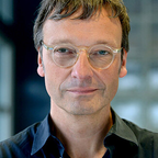
Martin Albrecht

Francesca Peiro Martinez
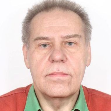

On nitride semiconductors, Pierre Ruterana has been carrying research for some 30 years, on the materials and devices. With some 100 invited lectures, more than 400 articles published in peer reviewed journals. Using high resolution transmission microscopy and atomistic multiscale modeling he has contributed to the determination of the atomic structure and properties of the defects in these materials. Most recent projects developed nitride based high power high frequency transistors which allowed to demonstrate cut off frequencies of 200 Ghz and working temperatures around 1000°. The emission across the green gap has always been an important topic, of course, bridging the green gap goes along with increasing the indium composition which introduces strain and leads to the degradation of the structural and crystalline quality of the devices. The objective, using high-resolution transmission electron microscopy, has always been to determine the mechanisms of such behaviour and collaborate with the growers in order to try to circumvent it and/or suggest ways for possible improvements.


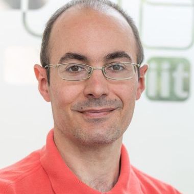
Giorgio Divitini received a Bachelor's and a Master's degree in Physics from the Universita' degli Studi di Milano in Milan, and a PhD in Materials Science at the University of Cambridge (UK). He was a post-doctoral researcher in the Department of Materials Science and Metallurgy for four years before taking on a position as Advanced TEM Officer in the same institution, working in the largest electron microscopy facility for physical sciences in Cambridge. In the summer of 2021 he moved to IIT to start a group dedicated to the advancement of electron microscopy and its applications.
Giorgio is passionate about pushing the boundaries of characterisation at the nanoscale, employing new detectors, new acquisition protocols and new data analysis approaches for electron microscopy and related techniques. His past work includes a variety of analytical techniques, including electron tomography, EDX and EEL spectroscopy, cryo-EM and in situ characterisation. Applications-wise, he has mostly worked on materials and devices relevant for energy, such as solar cells, LEDs and battery materials.

Paola Favia is a Principal Member of Technical Staff at Imec, Belgium. She holds a PhD in solid-state physics from the École Polytechnique Fédérale de Lausanne (EPFL), Switzerland.
Her research focuses on advanced electron microscopy methods for the quantitative characterization of semiconductor materials and devices, including TEM, STEM, 4D-STEM, iDPC, diffraction-based strain metrology, and EELS. She is particularly interested in strain analysis and multimodal microscopy to address the challenges of characterizing increasingly small and complex features.
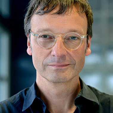
Martin Albrecht is Head of the Materials Science Department at the Leibniz-Institut für Kristallzüchtung (IKZ) in Berlin. He received his PhD in physics from the University of Hamburg in 1995 and worked at the University of Erlangen-Nürnberg, latterly as Assistant Professor, before joining IKZ in 2004 to lead its electron microscopy group. His research addresses the relationship between atomic-scale structure and the properties of semiconductors and functional oxides. Using quantitative STEM, analytical methods and in situ TEM, he studies defects, interfaces, alloy ordering, epitaxial growth and phase transformations, with particular emphasis on in situ TEM to follow structural evolution under relevant processing and operating conditions. Current materials of interest include III-nitrides, Ga₂O₃ and related oxides, and perovskite oxides. He leads the synthesis area of FAIRmat, the German national research data infrastructure for condensed-matter physics and the chemical physics of solids.

Francesca Peiró (PhD in Physics in 1993) currently serves as Head of the Department of Electronic and Biomedical Engineering and as researcher and member of the Steering Committee of the Institute of Nanoscience and Nanotechnology (IN2UB) at the University of Barcelona.
She coordinates the consolidated research group MIND (Micro-nanotechnologies and Nanoscopies for Electrophotonic Devices), and in particular the Laboratory of Electron Nanoscopies (LENS, https://lensgroupub.wordpress.com/), developing instrumental and data-processing methods for transmission electron microscopy and related analytical techniques applied to advanced nanomaterials. She is the scientific coordinator of the Barcelona node of the ICTS ELECMI (www.elecmi.es) dedicated to electron microscopy for materials science, fostering advanced aberration-corrected electron microscopy in Spain. She currently serves as President of the Spanish Society of Microscopy and is co-chair of the next European Microscopy Congress EMC2028 to be held in Barcelona (www.emc2028).
She has received the Jaume Vicens Vives Award for University Teaching Quality (2022) from the Generalitat de Catalunya, the Teaching Quality Distinction from the University of Barcelona's Social Council (2022), and the ICREA Academia Award (2023–2027).